Daily Log 2020-11-29: Finishing the sensing relay pcb
I've been working on and off on the pcb for my sensing relay project. Here were a few of the design challenges.
Cost
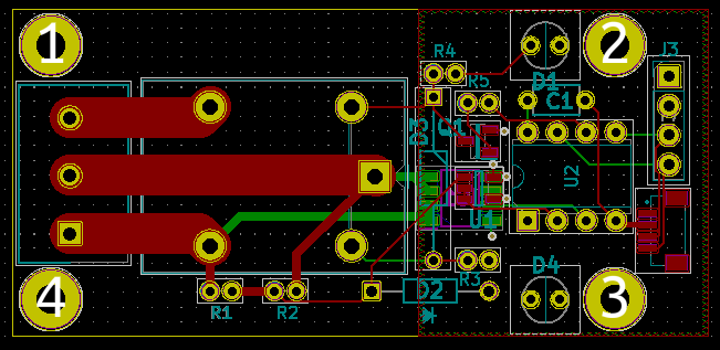
Cost is an obvious optimization dimension. For most board manufacturers the cost is directly proportional to the area of the board. That puts some pressure on ensuring that the design fits into the smallest area possible.
High power relay
The biggest challenge of the design is dealing with this high power relay. I'm hoping to have a safe operating range of 0 - 50V DC and 0 - 10A. That means a maximum power of 500W and that feels huge to me. One of the first things I was worried about was providing sufficient trace width between the terminal block and the relay. Traces are just little wires in a substrate, and so the same intuition that you have about wires (more current requires thicker wire) applies to traces as well.
In order to calculate the minimum trace width we need to know the maximum expected current the thickness of the traces. We already know we expect 10A but the thickness will depend on the manufacturing parameters. OshPark offers a special 2 layer 2oz board for high power applications (it also says it's thinner... so I hope that's not an issue). Using that and this trace width calculator we can plug these details in to see that we need 360mil traces. 1 mil is 1/1000th of an inch so this is roughly a third of an inch, this is HUGE, and frankly probably unachievable.
My current plan is to try running two 180 mil traces on both sides of the board. The traces should act like parallel wires each carrying half the load and so hopefully this works. I think that if this doesn't end up working (the result will be that traces will get too hot and melt) then maybe I can just try connecting the terminal and relay directly with some hefty 16AWG wire.
Another thing we have to worry about is giving sufficient spacing from the high voltage traces. However looking into what that would be for 50V it's still only a couple of mil and my safe trace distance of 4 - 5 mil is more than sufficient.
Lastly I've tried to separate the high voltage side from low voltage to prevent any leakage that could damage components and to make it clear to users what's safe to handle.
Relay RF Emissions
I've mentioned this a few times in previous logs but I'm thinking about the RF emissions from the relay opening and closing. When the coil gets opened and closed and there's a spray of RF from the magnetic field created from the inductor. This can impact other components, an early design I tried to place the hall effect sensor (current sensor) under the relay as it should be places as close to the current source as possible. However I ended up being nervous about the way that RF might impact the devices and put it further back in the low voltage side for safety.
The "Final" Design
This is the final v0 pcb layout that I intend to have printed. It will end up costing me about $4.50 to have it printed from OshPark. Along with the bill of materials that total cost per board should end up about $13.40.